Last month, Intel launched its 3rd Gen Xeon Scalable CPU family known as Cooper Lake based on the 14nm architecture. Now, some people in mainland China have got their hands on the first QS Cooper Lake chips which reveal an interesting design for the Cedar Island platform based family of LGA 4189 CPUs.
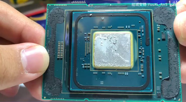
Intel 14nm Cooper Lake-SP Xeon QS CPU Delidded, Features 20 Cores on HCC Die & Gold-Plated Solder With Liquid Metal Thermal Compound
The person who posted this over at the Bilibili (via Momomo_US) states the this particular Cooper Lake-SP qualification sample is the Intel Xeon Gold 5320H. The CPU features 20 cores, 40 threads, based on the 14nm++ process node, and comes with a base clock of 2.2 GHz. As per the code over the IHS, this particular chip was produced all the way in 2019, around the beginning of August so it has been out since a year prior to the official launch in June 2020.
Now the official specifications for the Xeon Gold 5320H mention a base clock of 2.4 GHz & a boost clock of 4.3 GHz. The difference in clock speeds is once again due to the qualification nature of the chip itself which was made before the official specifications were finalized for the Cooper Lake-SP lineup. But the base clock isn’t the only change we see on this chip compared to its final retail form.
Just looking at the IHS, we see a striking resemblance to the older Cooper Lake (CPX-4) version than the Cooper Lake (CPX-6) version that was officially launched last month. The Intel Cooper Lake line was initially designed for both Cedar Island and Whitley platforms but the Whitley version (CPX-4) was later canned. We were expected to get up to 56 cores and 112 threads but Intel will now only be launching its 10nm Ice Lake-SP CPUs for the Whitley platform marking a huge update within the Xeon landscape since the launch of Skylake-SP all the way back in 2015.
A few more high-quality pictures of the Cooper Lake-SP QS CPU have been posted by the twitter user, Brutus (@brutuscat2):
Moving on, the chip was delidded too, revealing its dual-package design which is a common design choice used by Intel these days. The silicon lies on a separate package interposer that sits on top of the main PCB. Sitting next to the Xeon W-3175X, the Cooper Lake-SP looks much larger and that is also why it needs a larger socket (LGA 4189) to accommodate it compared to the last-gen Cascade Lake-SP Xeons (LGA 3647).
Other interesting details include the materials used to beneath the IHS which show a soldered design with gold solder and high-quality liquid metal thermal compound. We cannot say for sure if the retail variants also feature gold plated solder like this qualification chip. Considering that the competition already does it, I would go ahead and say that Cooper Lake-SP does utilize the same materials on the retail chips. The CPU also doesn’t share the same socket key as the official Cooper Lake-SP CPU. It’s more in line with the Whitley Platform’s socket key which confirms that this CPU is just one of the many abandoned Cooper Lake-SP (CXP-4) parts.
Another interesting detail that is exposed by this delid which would also otherwise remain hidden is the fact that the chip uses an HCC (High Core Count) die and not the XCC (Extreme Core Count) ones that allow for more than 18 cores. The HCC dies scale up to 18 cores but here you can see an HCC die used for a chip with 20 cores and 40 threads. There’s no explanation provided by the user regarding this and we don’t have proof if an HCC die with more than 18 cores exists or not.

Based on the pictures, the die seems nearly identical to the HCC die featured on Cascade Lake-SP chips. We aren’t sure how this is possible but this is what the user who has the chips in his hands has to say. The Intel Cooper Lake-SP Xeon CPU family is already on retail and shipping while Ice Lake-SP is expected to start shipping by the end of 2020.


