A picture of an experimental 48-core Intel CPU from 2009 used as a mock-up for upcoming Ice Lake CPUs.
Update: This leak has partially inaccurate information. Please refer to this exclusive for the full story.
A huge report from DigiTimes has leaked out claiming that Intel’s Ponte Vecchio GPU has found its home on TSMC’s lower-cost 6nm process. The leak originally sprung from a paywalled DigiTimes article and has since been corroborated by China Times as well in the last few hours. The implication of Intel shifting major products to TSMC is huge and the report even indicates that talks to move Intel’s bread and butter CPUs to the pure-play foundry are being held as well.
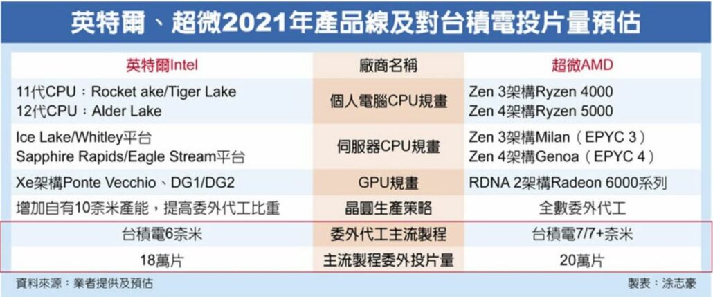
Intel’s Ponte Vecchio GPU will be made on the TSMC 6nm process, books 180,000 orders in advance
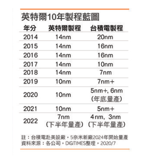
Intel’s 10nm process is actually better than TSMC’s 7nm process (MTr/mm2) and is roughly comparable to TSMC’s 6nm process. This means products that are fabricated on TSMC’s 6nm process (which is an optimized and lower cost version of 7nm) will have roughly the same density as a 10nm Intel part. This is problematic in the sense because Intel’s 7nm was supposed to have even higher MTr/mm2 and could impact the footprint of projects dependant on Ponte Vecchio such as the Aurora supercomputer.

Before we go any further, here is a translation from the relevant section of the DigiTimes article by @Chiakokhua and reproduced with permission:
Worth noting is, according to sources in the semiconductor industry, the volume for Intel’s GPU outsourced to TSMC in 2021 [i.e. Ponte Vecchio] is not high, and should be using the lower cost 6nm process. As for CPUs, plans for cooperation at the 5nm and 3nm nodes are currently in progress.
On the whole, although TSMC has made further inroads into securing Intel’s foundry outsourcing orders, the real volume will only happen in second half of 2022, and will be mainly about CPUs. As for GPUs to be introduced in 2021, if they are unable to compete favorably against NVIDIA and AMD, Intel may once again withdraw from the market, in which case there’s no orders to talk about.
Surprisingly, this also claims that Intel is planning to shift its bread and butter CPU parts to TSMC as well – although I want to make it clear that this part is not confirmed yet. This is something which, even after all things are said and done, we were not expecting. It is almost impossible to ensure consistency between two different foundries that are owned by different companies and don’t follow Intel’s Copy Exactly process. This likely means that Intel will decide to shift entire lineups to TSMC to ensure consistency. According to the Taiwanese publication, these are expected to be on the 5nm or 3nm process.

These findings were further corroborated by Chinatimes as well. The Chinese publication confirmed that TSMC’s 6nm process had received orders worth 180,000 wafers from Intel which will likely be used to manufacture Ponte Vecchio on a node that is roughly equal in terms of MTr/mm2 to Intel’s 10nm process. The report further mentions that AMD and Intel will be vying for wafer capacity as they battle it out for TSMC’s attention next year. A translation of the relevant portion is given below:
Computer processor makers Intel and AMD will battle for TSMC’s 7-nanometer-generation process capacity next year. The company (Intel) has reached an agreement with foundry leader TSMC to use TSMC’s 7nm optimized version of its 6nm process for mass production of processors or graphic chips starting next year.
In the second half of this year, TSMC began converting some of its 7nm capacity to 6nm, and will enter mass production by the end of this year. The market had expected TSMC to receive fewer orders from Huawei and Hess, resulting in a shortage of capacity for TSMC’s 7nm process next year. However, with Intel confirming to outsource and book 6nm capacity next year, and Supermicro expanding orders to cover most of its 7/7+nm capacity, TSMC’s advanced processes will remain at full capacity in the first half of next year, resulting in a slow first quarter of operations.
Intel’s 10nm transistor volume (MTr/mm2) is slightly better than TSMC’s 7nm and comparable to TSMC’s 6nm, according to equipment industry sources, and in the second half of the year the two companies will begin working together to redesign the photomasks on some of Intel’s 10nm processors or graphics chips to conform to TSMC’s processes.
Intel has reached an agreement with TSMC and has ordered 180,000 wafers of TSMC’s 6-nanometer production capacity for next year, the company said.
This would also explain the rumors we saw earlier about NVIDIA shifting their GPUs to Samsung’s 8nm process. With Intel and AMD both slugging it out for capacity, there [opinion] probably isn’t enough room for another company [/opinion] and it would make sense for green to move to a foundry with more breathing room. This also has interesting implications for the future of Intel’s TMG efforts and the increasing importance of TSMC as the flagship foundry of the world.
Ponte Vecchio is a very important milestone for the company, and if it had to tap TSMC to fab it properly (and that too at a lower density node), it raises questions on the efficacy of TMG – which has now delayed two processes in a row. Hopefully, they get their house in order soon, because we need Intel to keep applying competitive pressures to the industry and driving transistor density forward.


