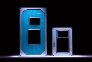
A day ago we covered a report from DigiTimes stating that Intel had booked 180,000 wafers on their 6nm process and would be using the node for their flagship HPC Ponte Vecchio GPU. Well, as it turns out, DigiTimes got the order right (more on that later) but were completely off the mark about the product. Intel’s Ponte Vecchio GPU will not be manufactured on TSMC’s 6nm process. Instead, it will be made concurrently on both TSMC’s 5nm and Intel’s 7nm process.
Intel’s Ponte Vecchio GPU will be made concurrently on Intel 7nm and TSMC 5nm
Intel’s PVC GPU is the company’s flagship effort for discrete graphics and is going to be in a starring role in the upcoming Aurora supercomputer. So it is not surprising that investors were spooked when they heard Intel’s CEO accepting that the company will be relying on TSMC more in an effort to compliment their own foundries. Two seperate publications then reported that Intel’s PVC GPU is going to be manufactured on the TSMC 6nm process which was even more surprising because T6 is essentially an optimized variant of T7 which is roughly equal in density to Intel’s 10nm process. Such a shift would drastically alter the power profile of Intel’s upcoming GPU.
So we independently reached out to a couple of sources in Taiwan and got the facts first hand from people directly involved in the making of this GPU. Here are the facts (cross-referenced from each source to verify their validity):
- TSMC’s 5nm process is roughly comparable in density to Intel’s 7nm process and PVC is only feasible at that density level – so 6nm (which is an optimized process for TSMC 7nm) is out of the question.
- Ponte Vecchio will have multiple SKUs.
- All PVC SKUs will have an IO die made at Intel.
- Compute dies will be made either on Intel’s 7nm process or TSMC’s 5nm process depending on the exact SKU.
- The Rambo cache will be made in-house at Intel as well.
- The connectivity die (Intel Xe) was originally intended to be built over at TSMC and will remain that way.
- Intel did place an order worth 180,000 wafers on the TSMC 6nm process but it is not related to PVC and is part of their ongoing partnership (Intel has been using TSMC for quite a long time).
So there you have it. While the Taiwanese newspapers were right about the wafer order, they were wrong in believing it is about PVC. That order is not related to Ponte Vecchio at all which requires a process with a density that is greater than TSMC 7nm/6nm and/or Intel 10nm. If you are only interested in the world of facts and don’t want to venture into the murky yet dreamy territory of educated speculation, stop now.
[speculation] It does beg the question though: will we see a TSMC 5nm flavored PVC SKU before an Intel one? That is something that could very well happen considering Intel’s 7nm has been delayed and TSMC’s 5nm process remains on track to arrive by 2021. In either case, we will likely not see volume on PVC parts before 2022. [/speculation]
I would also like to point out that this is the state of things as they currently stand, should Intel magically fix their 7nm process and get back on track – things might move around a little. Intel’s deleted tweet stated that the company is planning a big reveal soon and I have a feeling we might get a ton of information when that happens – and further clarity on their Xe efforts.


