More rumors have emerged on AMD’s RDNA 2 “Navi 2X” GPUs which will be powering the next-gen Radeon RX line of graphics cards. The rumor once again suggests a late Q4 2020 launch & also talks about RDNA 3 and how it aims to be one of the biggest revolution for GPUs by the time it launches.
AMD Radeon RX Navi 2X ‘RDNA 2’ GPU Rumors: No HBM2, Earliest Launch in November, 7nm+ For Enthusiast & Mainstream GPUs
The rumored information comes from AquariusZi (via @davideneco) who is a well-known name in the tech scene at the PTT forums. The user was the first to list down expected die sizes of AMD’s RDNA 2 GPUs and has now shed some more light on what we can expect from the upcoming Navi 2X line of GPUs for next-generation Radeon RX graphics cards.
AMD’s First RDNA 2 GPU, Big Navi, Is Expected For Launch in November But No AIB Partners Have The Chip Yet
This is the second rumor which seems to suggest that AMD’s first RDNA 2 GPU or Big Navi for the Radeon RX graphics card segment will be introduced in Q4 2020. The source points out the launch in November 2020 and also mentions that there are no orders for the Navi GPU yet which reveals that we might only get a reference flavor at launch with custom boards arriving months later.
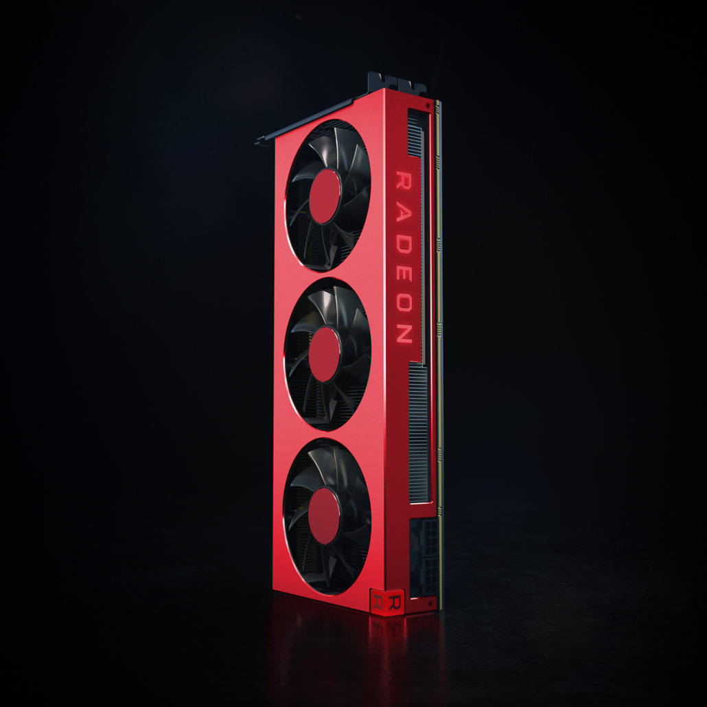
Based on this information, it seems like that AIBs would miss out on the launch window for offering their custom designs for Big Navi. Meanwhile, NVIDIA custom designs for its next-gen Ampere GPU lineup have already leaked out. Considering that this is AMD’s flagship part, the reference design will have to be solid enough to give enthusiasts a reason to buy it at launch or they would have to wait for custom variants to arrive with no specific launch date. Some users could simply grab the reference variants and wait till water block manufacturers deliver their own cooling blocks for the Big Navi GPU.
AMD’s RDNA 2 Gaming GPU Lineup Won’t Feature HBM2 Memory or 2.5D Design
The second bit of information is regarding the memory design and the source says that RDNA 2 GPUs, at least the gaming variants, will not be getting HBM2 memory or a 2.5D design. Earlier, it was reported that Big Navi GPU based Radeon RX graphics cards would feature 16 GB of GDDR6 memory along a 512-bit bus interface. This would essentially double the memory capacity & bus size over Navi 10.
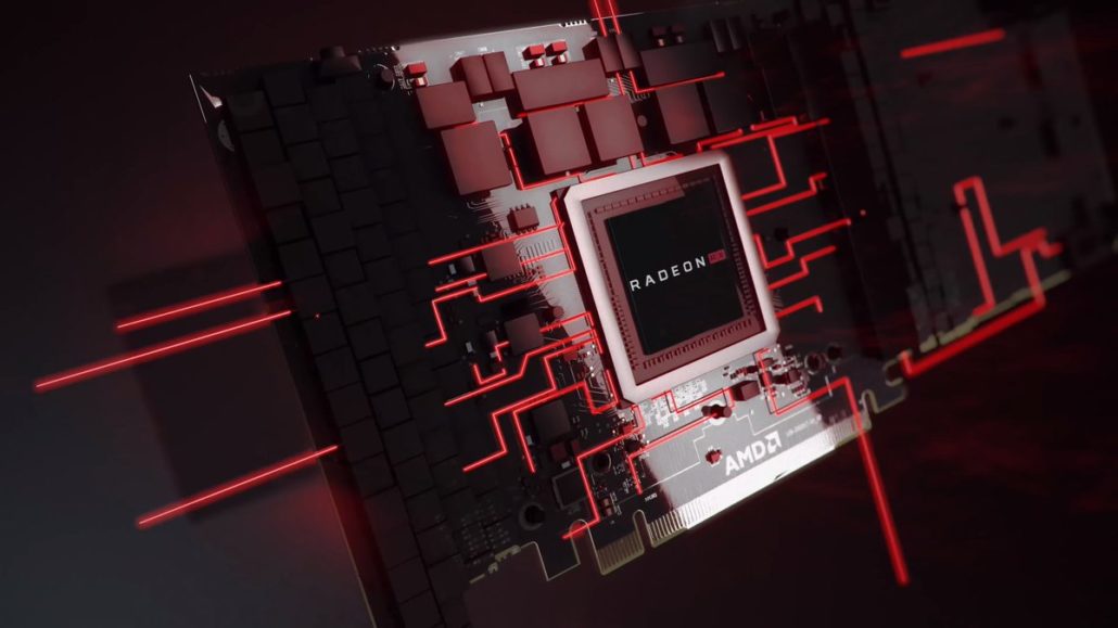
At the same time, there have been references within AMD’s GPU drivers which suggest HBM2 memory for AMD’s Big Navi GPUs. Spotted by FreeDesktop (via Videocardz), it is mentioned that a 2048-bit bus interface may happen however this would suggest two variants of the Big Navi GPU since HBM2 memory requires a 2.5D design leading to a vastly different chip design due to the different memory controllers.
It is highly likely that AMD will retain GDDR6 for its next-generation RDNA 2 gaming graphics cards but we may see a workstation or prosumer tuned variant with HBM2 memory. Again, this is just a theory at this point and I will personally stick with GDDR6 for Big Navi.
AMD’s Enthusiast & Mainstream RDNA 2 GPUs Will Utilize The TSMC 7nm+ Process Node?
One thing that AMD hasn’t made it very clear till now is what process node would the RDNA 2 GPUs utilize. While AMD’s Zen 3 is confirmed for 7nm+, the RDNA 2 GPUs are mentioned on 7nm process node since the earliest of roadmaps however AMD has since pointed out that just like the Zen CPU updated roadmap, 7nm doesn’t mean that it can’t be an enhanced version of the node.
According to AquariusZi, AMD’s flagship and mainstream RDNA 2 GPUs will utilize the TSMC 7nm+ process node. He also mentions the entry-level Navi GPU but doesn’t mention what node it would utilize.
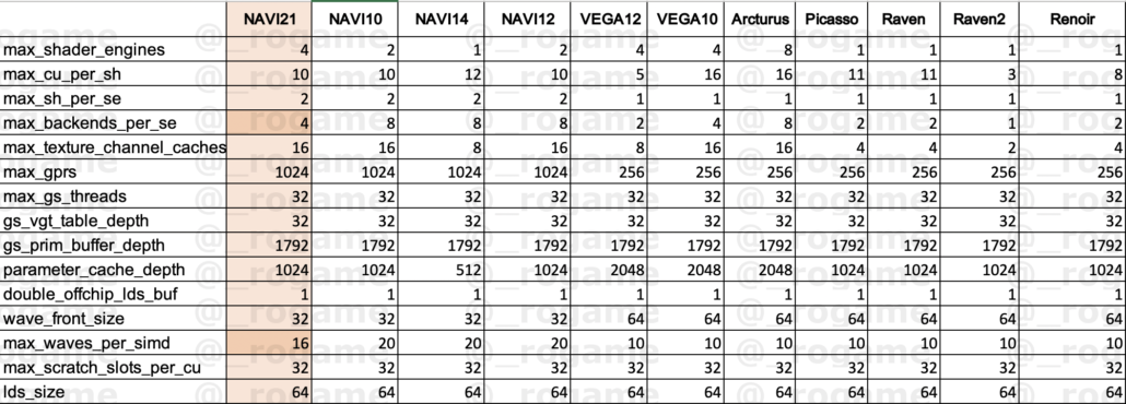
In addition to all of the rumored details, Rogame managed to provide the latest GPU configuration for the Big Navi chip. Once again, the GPU is suggested to feature 80 compute units of 5120 cores. We took a more detailed look at the leaked specifications here.
AMD Big Navi Radeon RX GPU ‘Speculated’ Specifcations:
| Graphics Card | Radeon RX Vega 64 | Radeon VII | Radeon RX 5700 XT | Radeon RX ‘Big Navi’ |
|---|---|---|---|---|
| GPU Architecture | 14nm Vega (Vega 1st Gen) | 7nm Vega (Vega 2nd Gen) | 7nm Navi (RDNA 1st Gen) | 7nm+ Navi (RDNA 2nd Gen)? |
| Compute Units | 64 | 60 | 40 | 80? |
| Stream Processors | 4096 SPs | 3840 SPs | 2560 SPs | 5120 SPs? |
| TMUs / ROPs | 256 / 64 | 240 / 64 | 160 / 64 | 320 / 64? |
| Base Clock | 1247 MHz | 1400 MHz | 1605 MHz | TBD |
| Boost Clock | 1546 MHz | 1802 MHz | 1905 MHz | TBD |
| Game Clock | ~1450 MHz | 1750 MHz | 1755 MHz | TBD |
| Compute Power | 12.66 TFLOPs | 13.44 TFLOPs | 9.75 TFLOPs | TBD |
| VRAM | 8 GB HBM2 | 16 GB HBM2 | 8 GB GDDR6 | 16 GB GDDR6? |
| Bus Interface | 2048-bit | 4096-bit | 256-bit | 512-bit |
| Bandwidth | 484 GB/s | 1024 GB/s | 448 GB/s | 896-1024 GB/s? |
| TBP | 295W | 295W | 225W | 250-300W? |
| Price | $499 US | $699 US | $399 US | TBD |
| Launch | 7th August, 2017 | 7th February, 2019 | 7th July 2019 | November 2020? |
AMD’s Next-Generation RDNA 3 GPUs To Feature Revolutionary Chiplet Design
Lastly, the rumor points out AMD’s next-generation RDNA 3 GPUs and mentions that the GPU is currently in the early design and test phase but will feature the most revolutionary GPU design in the form of a chiplet architecture. The RDNA 3 chips will bring the same design methodology as Zen 2 but for GPUs, allowing AMD to mix and match several GPU IPs together.
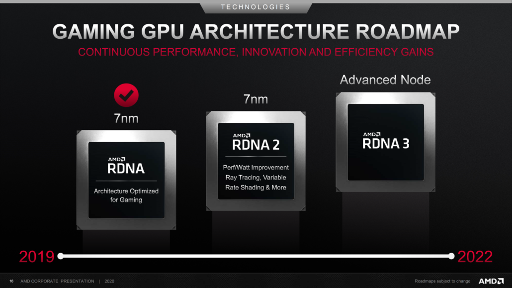
The most interesting part in all of this is that the source doesn’t mention a specific node but calls out the ‘Advanced Node’ as more of a technical term where AMD will utilize several different nodes for the various chiplets embedded on the same interposer. There’s a likelihood that AMD will be separating the main graphics dies from the I/O dies like Zen 2.
We can see the I/O such as memory controllers and other IPs featured on different nodes than the main GPU dies. It’s too early to talk about RDNA 3 GPUs at the moment but we can expect to hear more on AMD’s chiplet endeavors for the GPU side in 2021 with an expected launch in 2022.


