A featured image of the NVIDIA GA100 die.
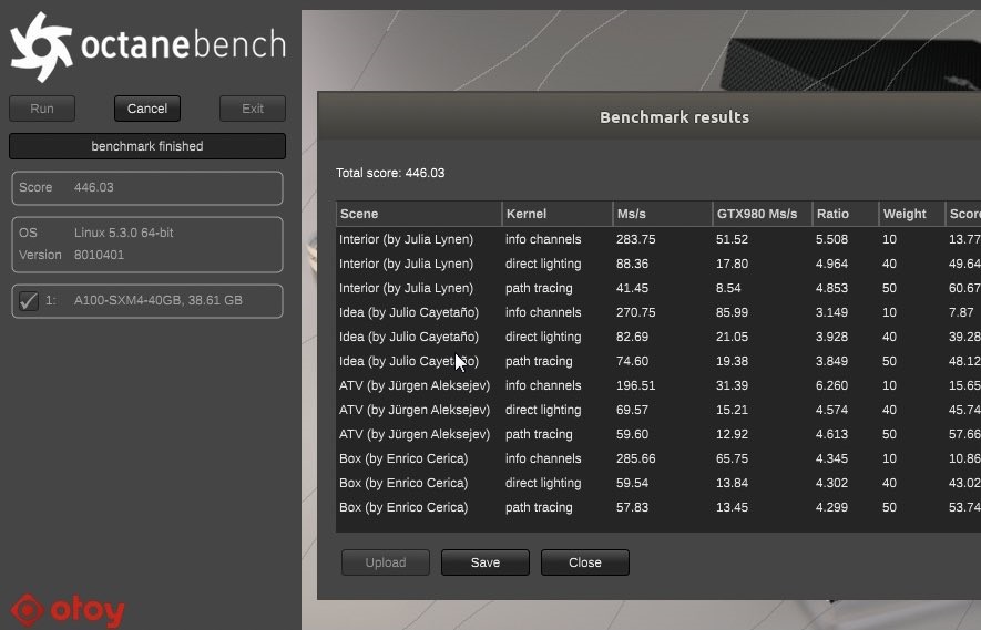
While we wait for consumer graphics cards based on the Ampere GPU architecture to launch, NVIDIA’s flagship Ampere chip, the A100, continues to break world records. The world’s largest graphics chip based on the 7nm process node was unveiled back in May and has big numbers backing it up when it comes to specifications and performance. The Ampere A100 tensor core accelerator has now become the fastest GPU ever recorded on OctaBench.
NVIDIA Ampere A100 HPC Tensor Core GPU Becomes The Fastest GPU Ever Recorded in Octa Bench, Delivers 43% Better Performance Than Turing With RTX Off
The feat was shared by the CEO of OTOY, Jules Urbach. OTOY are the developers behind Octa Bench which is a benchmark tool that lets users evaluate GPU performance using the Octane Renderer. OctaneRenderer itself is a GPU render engine that supports NVIDIA’s RTX raytracing hardware acceleration to deliver crisply rendered scenes.
According to Jules, the NVIDIA A100 Tensor Core GPU posted a score of 446 in the OctaBench. He also states that this score is on average 43% faster than the Turing GPU in OctaneRender even with RTX Off. The Turing results compared here utilize RTX and unlike games that cause a significant drop in frame rate, enabling RTX within the OctaRenderer leads to better performance since scenes can be rendered and finished faster with the available ray tracing hardware.

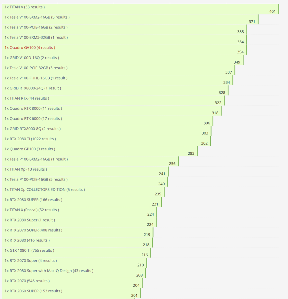
It isn’t stated which exact Turing GPU was used for comparison against the NVIDIA Ampere A100 GPU but looking at the complete average benches of all cards tested, we see a range of interesting results. On average, the Tesla V100, the A100 predecessor, is about 20% slower but for some odd reason, the Titan V is only 11% slower which is surprising considering the Titan RTX is 38% slower than the A100 GPU.
The main answer to this could be the fact that the Titan V leverages the same GV100 GPU as the Tesla V100 which could be more optimized towards this datacenter and cloud-scale benchmark whereas the Turing GPUs are more optimized towards gaming and GP-GPU use. But then again, the CEO of the company states that this is the fastest GPU ever recorded on the specific workload which is a big feat for NVIDIA’s A100 GPU accelerator.

The NVIDIA A100 is by far the largest 7nm chip produced to date, featuring a gargantuan 54 Billion transistors packed within a single die. The A100 comes with a vastly cut-down configuration due to early yields but like the Tesla V100, we could see a higher bin version with more cores once yields do improve and that would further increase the performance in this specific benchmark.
The full implementation of the NVIDIA Ampere GA100 GPU includes the following units:
- 8 GPCs, 8 TPCs/GPC, 2 SMs/TPC, 16 SMs/GPC, 128 SMs per full GPU
- 64 FP32 CUDA Cores/SM, 8192 FP32 CUDA Cores per full GPU
- 4 third-generation Tensor Cores/SM, 512 third-generation Tensor Cores per full GPU
- 6 HBM2 stacks, 12 512-bit memory controllers
The A100 Tensor Core GPU implementation of the NVIDIA Ampere GA100 GPU includes the following units:
- 7 GPCs, 7 or 8 TPCs/GPC, 2 SMs/TPC, up to 16 SMs/GPC, 108 SMs
- 64 FP32 CUDA Cores/SM, 6912 FP32 CUDA Cores per GPU
- 4 third-generation Tensor Cores/SM, 432 third-generation Tensor Cores per GPU
- 5 HBM2 stacks, 10 512-bit memory controllers
One can only imagine what the performance metrics would be once the Ampere cards with RTX enabled are brought to market. If this specific benchmark is anything to go by, then we can see Ampere GeForce RTX 30 series cards easily coming in close to their HPC counterparts.


